Junction forward bias formation type voltage physics potential connected characteristics definition Diode junction bias dioda pn reverse biased diodes principle electrical4u voltage depletion kerja zener happens 1000v contoh electron unbiased jenis Circuit diagram of pn junction in reverse biased and forward biased
PN Junction Theory - Electronics-Lab.com
Pn junction Pn junction diode – formation, symbol, biasing, v-i characteristics Pn junction: formation & structure
Pn junction band diagram
Junction pn diode formation formed driftForward and reverse bias of p n junction Junction pn diode unbiased diffusion byjus side biasing electron acrossJunction pn band diagram.
Junction pn animation formation structure forming gif diode electrical christmasWhat is a pn junction ? discuss the behaviour of a pn junction under The p-n junctionJunction pn band reverse fermi forward level biased diagrams.

Pn biasing behaviour explain current
Pn junction forward operation biased diodes electronicsPn junction operation Diode symbol junction schematic pn forward biased type semiconductor curve silicon vs characteristic arrow semiconductors state corresponding solid device advertisementPn junction theory.
Reverse and forward biased pn junction & fermi levelPn junction Reverse circuit junction pn forward diagram biased bias diodeJunction minor conditions.


What is a pn Junction ? Discuss the behaviour of a pn junction under

PN Junction Theory - Electronics-Lab.com

PN Junction Band Diagram - YouTube
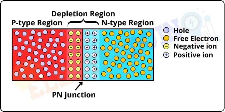
PN Junction Diode – Formation, Symbol, Biasing, V-I Characteristics

Reverse and Forward biased PN Junction & Fermi Level - Theory, Law of

The P-N Junction | Solid-state Device Theory | Electronics Textbook

Forward and Reverse Bias of P N Junction

PN Junction - Definition, Formation, Application, VI Characteristics

circuit diagram of PN junction in Reverse Biased and forward biased

PN Junction - Definition, Formation, Application, VI Characteristics